Full-custom 8-bit R-2R DAC with layout-level optimization
Full custom design of an 8-bit R-2R Digital-to-Analog Converter (DAC) with control over gate placement, routing, and layout-level optimization; designed and sized an Operational Transconductance Amplifier (OTA).
Case Study
Problem
Design an 8-bit Digital-to-Analog Converter from the transistor level, meeting specs for linearity, bandwidth, and noise in a real 180 nm process.
Architecture
- R-2R resistor ladder network for binary-weighted current summation
- Custom Operational Transconductance Amplifier (OTA) for output buffering
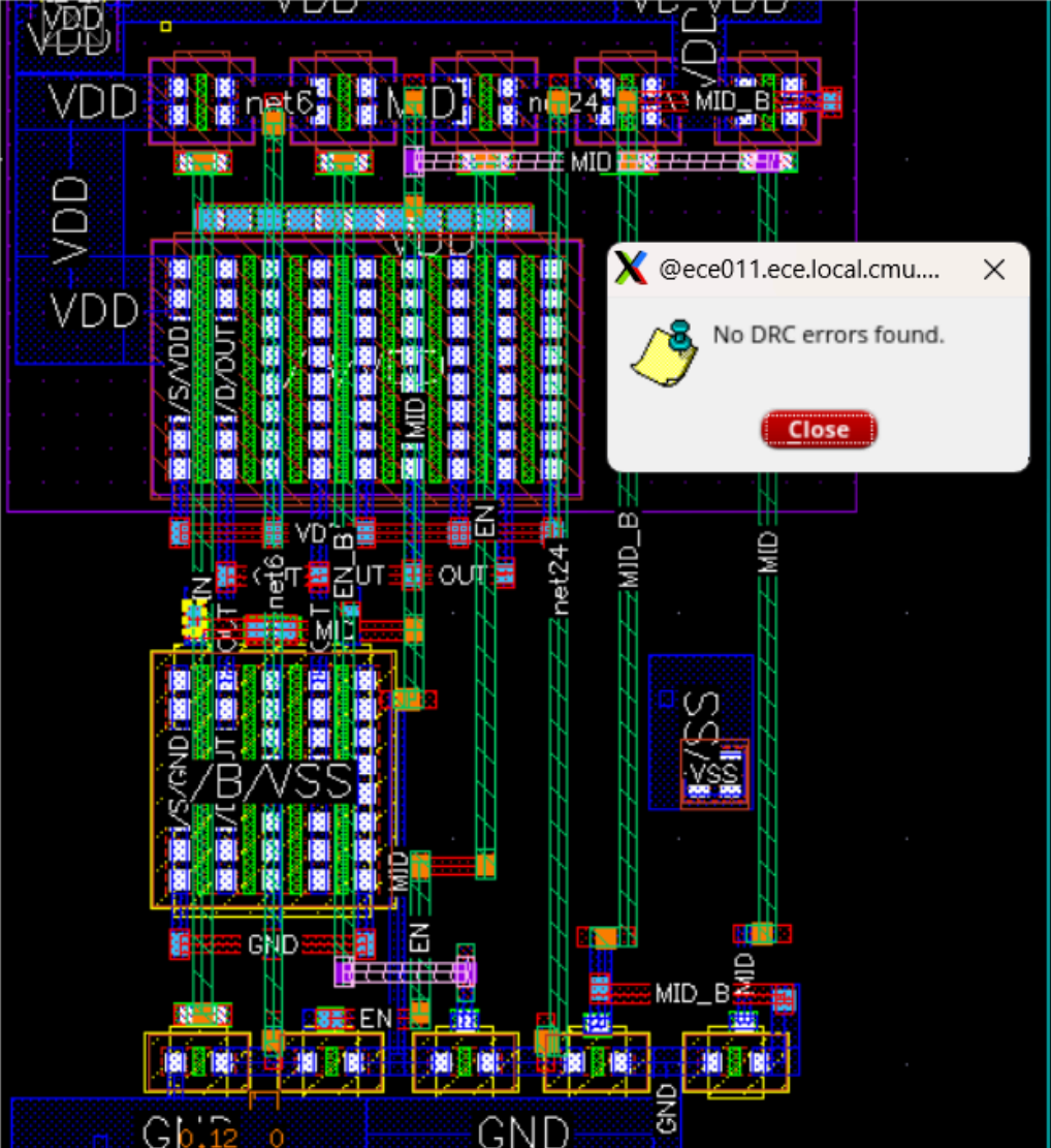
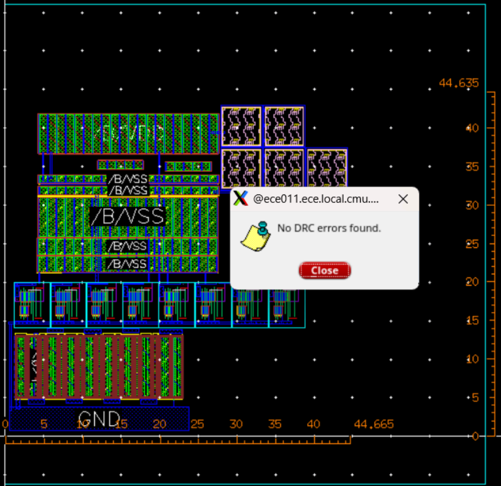
- Full Cadence Virtuoso schematic with manual gate placement and routing
- Parasitic extraction and post-layout simulation to verify AC/DC specs
- DRC and LVS sign-off for physical design rule compliance
Challenges
- Meeting gain-bandwidth requirements with the OTA across PVT corners
- Minimising layout-induced mismatch in the R-2R ladder for DNL/INL targets
- Routing high-density analog layout without introducing parasitic coupling
- Iterating schematic ↔ layout ↔ simulation without breaking convergence
Tradeoffs
- Chose R-2R topology over current-steering DAC for simpler layout at 8-bit resolution
- Sized OTA for 70 dB gain over 1 MHz bandwidth; narrower than some alternatives but sufficient for audio range
- Manual routing prioritised matching over density to protect linearity
Outcome
Passing DRC/LVS; post-layout simulation met DNL < 0.5 LSB and INL < 1 LSB across nominal and SS process corners.
What I Learned
- Full-custom analog IC design flow from schematic to layout sign-off
- OTA topology selection and sizing methodology (gm/ID approach)
- How parasitic extraction changes AC response vs schematic simulation
- Cadence Virtuoso layout techniques for matching-sensitive analog circuits